Back in April I mentioned that we’d been working on a number of fun projects and one of those involves an early 1980s vintage scanning electron microscope (SEM), which we don’t really have a use for, but sometimes when a bargain — it cost less than you’d pay for the vacuum system on eBay — comes your way, it’s hard to resist.
Given that none of us have any prior experience operating (let alone maintaining!) an SEM, it’s already turned out to be a fun learning experience. There are also one or two hacks that we have in mind, but more on this later. And, you never know, one day it may well actually prove useful to have the ability to produce particularly high resolution and depth of field images of samples on-site.
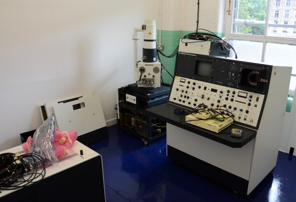
Components
In the image at the top of this post you can see:
- Main electronics cabinet (large unit to the right)
- Electron column and sample chamber (to the left of the main electronics)
- EDS computer (bottom-left)
For all intents and purposes it’s an analogue machine, using a black and white TV CRT for setup and finding the area of interest, with a second, circular, intense blue phosphor CRT or “high resolution record unit”, that has a 4,000 line slow scan capability and onto which you would attach a Polaroid or 35mm film camera. However, a simple frame store with some image processing capabilities was also later added and can be seen sat on the “table” attached to the main cabinet.
Directly underneath the sample chamber there is a turbomolecular pump, which is backed by a rotary vane vacuum pump located behind it. On the door of the chamber there are 3 large knobs for manually adjusting sample stage X, Y and Z position. However, this SEM was also upgraded with electronic position control and so these attach to small stepper motors, which are driven via a joystick and the smaller cabinet pictured sat on top of the main electronics unit.
The computer pictured bottom-left is part of the energy-dispersive X-ray spectroscopy (EDS) add-on, that allows the abundance and distribution of elements in the sample to be mapped. This connects up to the main cabinet and also to a liquid nitrogen cooled silicon X-ray detector, which is not pictured, but is affixed to a port on the side of the sample chamber.
Other add-ons not pictured include a cathodoluminescence detector for analysing the light given off by samples when bombarded by electrons (e.g. geological samples with luminescent minerals), and a speciment current amplifier, which can be used to image semiconductors in operation.
A steep learning curve

The SEM came with quite a lot of documentation and the seller was kind enough to label those cables that were not already labelled. However, after having been shook around in the back of a van over the course the few hundred miles journey to its new home, the aged yellow paper labels fell off a good number of the cables which had been labelled many years previous. Fortunately, these were limited in number and most had proper cable markers which had been applied at the factory.
In addition to an element of cabling ambiguity, there was also the question of how to know when it’s operating correctly; an SEM is nothing like a simple light microscope to operate, there are lots of variables and plenty of reasons why you might not be getting an image. Fortunately, Ken Swanson of Tron Tech — who previously worked for the manufacturer, installed the machine at its original owners and went on to service it for many years following — was generous in offering advice, without which it would likely have taken a great deal longer to get up and running.

One particularly invaluable piece of advice given was for a method of finding the rough starting X + Y micrometer positions for aligning the electron column final aperture. The SEM has four of these, each perhaps a couple of millimetres in diameter and with a precision drilled hole in the middle, the diameter of which is measured in microns. There is an electronic aid for tuning the position once you’ve got an electron beam through the aperture, but first you need to get near and just twiddling the micrometers at random with the apertures fitted is like finding a needle in a haystack. It seems obvious now, but temporarily removing one to expose a much larger hole makes the job a lot easier — and it does also help by being told roughly where to look.
First results
After a great deal of reading, advice, removing PCBs and cleaning edge connectors, trying and re-trying, some pretty encouraging results were obtained. The above video shows the B&W CRT with the SEM set to TV display mode, a graph mode focus aid, and other operating modes.
Next steps
While the SEM now works the performance could be better and there are intermittent faults, plus various general improvements that could be made, such as the addition of digital image acquisition and computer control of sample stage positioning. These are just some of the things I plan to cover as part of a new series of posts over on DesignSpark and I’ll add links here in due course.
Updates
- 28/07/16 — SEM Adventures Pt. 1: Introducing the Machine
- 01/08/16 — SEM Adventures Pt. 2: Cooling and PSU Overhaul

Andrew Back has in excess of 20 years industry experience that spans IT infrastructure, telecommunications and electronics, and covering R&D through to architecture, strategy and governance.