Reverse engineering is often a high-tech, expensive endeavour – but David Freitag’s latest project takes it down to the bare essentials, attacking a USB 3.0 eMMC reader board with nothing more than a desoldering station, sandpaper, and a flatbed scanner.
“Say there’s a Chinese silicon vendor which designs and sells a chip that does a lot of really fancy stuff. You’re super interested because said fancy bits can be had for the low low price of a few hundred pennies. Awesome, you might say, lets buy them! But there’s an issue,” David explains of the reason for his needing to reverse engineer a four-layer printed circuit board. “Documentation. Silicon vendors, Chinese or otherwise, have a nasty habit of making it nearly impossible to find proper documentation for a specific product; whether it’s poorly documented, NDA’d, or in some cases simply nonexistent.”
While the obvious fix would be for vendors to improve their documentation, possibly even to make their development hardware and reference designs available under an open source hardware licence, David’s approach requires no cooperation from the vendor – but it does require a certain amount of care, a lot of patience, and a steady hand with 600-grit sandpaper.
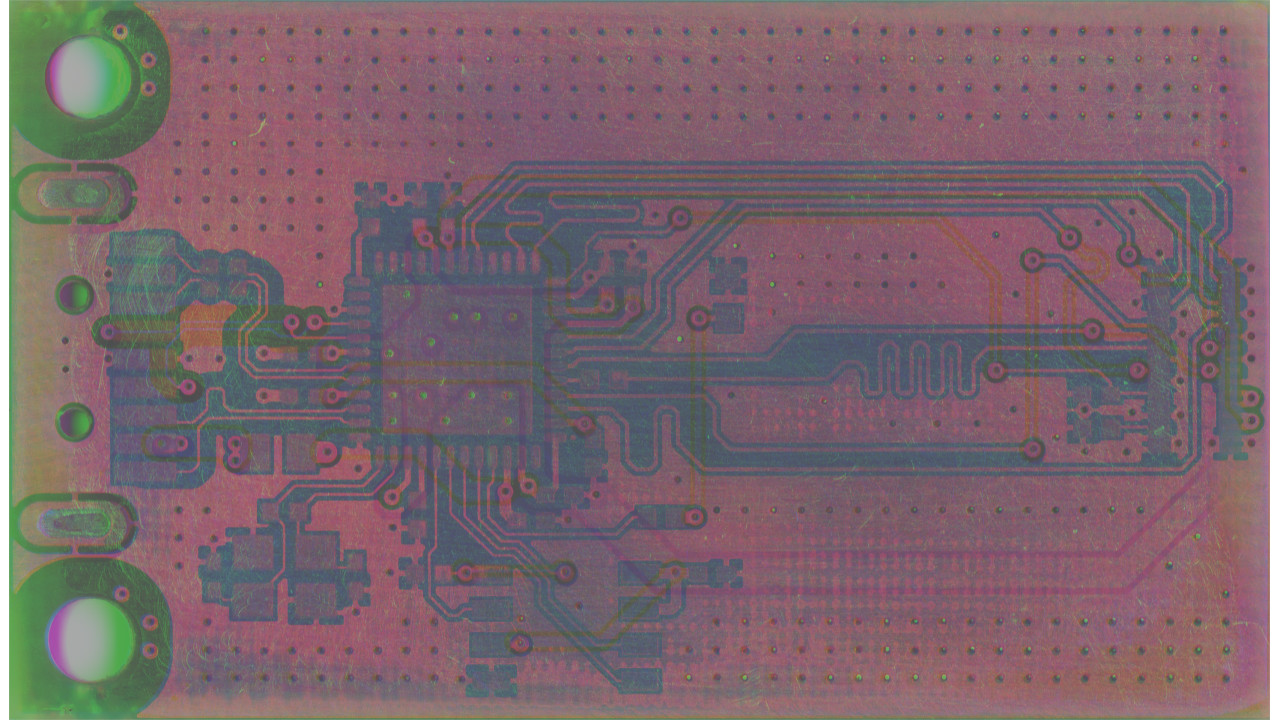
“You’re going to need some hot air reworking tools and a relatively high DPI scanner,” David explains, showing how the hot-air station can be used to remove larger components and the scanner to take high-resolution imagery of the two exposed layers of the PCB. The sandpaper, then, comes in handy to remove first the soldermask and then the upper layers of the PCB to expose the two hidden, inner layers and their traces.
“Once you have exposed layer 3 (which in this case was frustratingly only solid ground pour), take all of your scans and composite them,” David continues, showcasing how the scans can be combined into an image which makes clear which layer each trace belongs to and where it goes. “Set each layer to a pure color by dumping the saturation and tweaking with the layer opacity until you get something you can understand.”
The full process, along with the in-progress and final images and links to David’s work-in-progress schematic and Eagle library, can be found on 801labs.org.

Gareth Halfacree is a technology journalist and technical author best known for his work on the Raspberry Pi User Guide and an upcoming book covering the BBC’s micro:bit project. A keen open source advocate and RISC-V fan, Gareth is responsible for curating our fortnightly community round-up posts.