The cause of truly home-made semiconductors hit a major milestone late last month when engineer Sam Zeloof became, to common knowledge, the first person to successfully create an integrated circuit using a fully photolithographic process in a home lab, building a dual differential amplifier using entirely homebrew equipment.
Hobbyists around the world have been making discrete circuits at home for years, but integrated circuits are a significantly trickier matter. Engineers like Jeri Ellsworth have succeeded in the past using conductive epoxy and other tricks for the on-chip interconnects, but Sam’s work is the first to use a photolithographic process – the means by which modern IC are created, traditionally involving an expensive cleanroom environment with even more expensive photolithographic equipment.
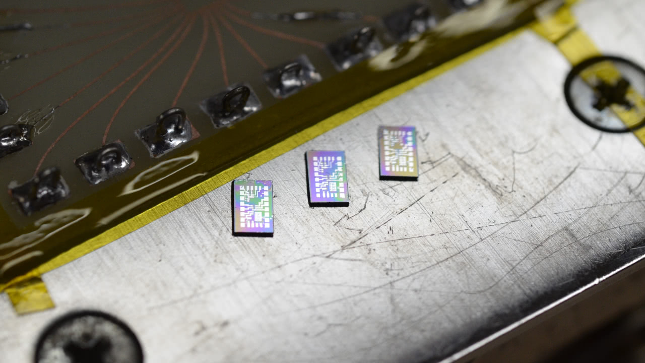
In a write-up of Sam’s achievement on Hackaday, the process is explained in brief: use of a converted digital light panel (DLP) projector for ultraviolet photolithography and an electron microscope for electron-beam lithography, and sputtered aluminium for on-chip interconnects. While still not exactly within reach of your average hobbyist, Sam’s work demonstrates that it is possible – with time and ingenuity – to build photolithographic ICs in a garage environment.
More information on Sam’s work, including a full write-up of his first successful IC output, is available on his personal blog.
For those who would prefer to have their custom chips made outside the garage, Colombia-based OnChip has unveiled an open-source platform which aims to do for custom semiconductor creation what services like OSH Park have done for circuit boards: Itsy-Chipsy.
“Chip prototyping used to be prohibitive for small start-ups and academy until services like MOSIS brought down prices to few thousands dollars per mm² in technology nodes capable to run circuitry at moderated performance,” OnChip explains of the current state of the semiconductor art. “MOSIS runs a multi-project wafer service that aggregates multiple designs onto one mask set to reduce prototyping costs. This aggregation restricts minimum sizing to few millimetres bringing down prices from hundred thousand to few thousand dollars.
“However, as an example, five thousand dollars budget for a college in a developing country might be a big number. It is definitely a huge number for a tinkerer or an engineer student ambitious enough to leap from the discrete world to the integrated planet. A service capable to deliver a chip for hundred dollars would break a paradigm and place a bridge to a community always hungry of new chips.”
Enter Itsy-Chipsy, a chip platform with regulators, voltage references, current sources, SPI, JTAG, clock generators, temperature and process monitors, a pad library – all the core utility functions of a modern semiconductor. “These utility blocks are placed on the chip to service blocks designed by users of the service,” OnChip explains. “With this chip platform, we paved the way to a multi-block service – like OSH Park – capable to offer silicon area for your own chip, for as low as hundred dollars.”
The second generation of the platform is in progress now, OnChip reports, with demonstrable prototypes expected by September this year and a target cost of around $350 per 350µm² block implemented in 180nm CMOS nodes and the potential to split a block in four to bring the price of a finished relatively simple DIP40 or dual QFN packaged design below the magic $100 mark.
More information is available on the project’s Hackaday page.
The Open Source Hardware User Group (OSHUG) has announced the schedule for OSHCamp 2018, to take place in Lincoln’s The Blue Room on the 30th of June and 1st July.
Announced via a call for participation back in January, the Open Source Hardware Camp (OSHCamp) 2018 is to take place in Lincoln, once home to noted engine builders Ruston & Hornsby – a company which still lives on as Siemens, following a route via GEC and English Electric. As with previous years, OSHCamp 2018 is split across two days: talks on Saturday the 30th of June, with a social event that evening, and hands-on workshops on Sunday the 1st of July.
Confirmed talks for the Saturday include Dr. Graham Markall on cycle-accurate simulation in the Verilog hardware description language, Tony Brookes on high-altitude balloon communications via LoRaWAN, Alan Wood on machine vision, Derek Woodroffe on the creation of electronic Tesla coils, Spencer Owen on how to transition from hobby project to functional business, Anna Sera Lowe on the MakerNet Alliance, James Pawson on electromagnetic compatibility testing for the Internet of Things (IoT), Jonny Edwards on non-standard computation, Damon Hart-Davis on “heating as a service” via technological and societal measures, and Giulio Moro on the ultra-low-latency audio and sensor processing platform Bela.
Workshops on the Sunday include a RISC-V quickstart, an introduction to NetBSD on embedded platforms, an in-depth exploration of high-altitude ballooning, a machine vision project, a Bela hands-on, a two-hour build of the RC2014 Mini Z80 Retro Computer, sold at a discount during the event, and the traditional soldering workshop.
More information on the event, including travel and accommodation details, can be found on the official website and the event discussion list.
The Global System for Mobile Communications Association (GSMA) has announced that its planned universal embedded subscriber identity module (eSIM) standard is being postponed, following the launch of an investigation by the US Department of Justice into alleged mobile network collusion designed to throw the technology off track.
First introduced in principle by the GSMA in 2010, embedded SIMs (eSIMs) replace the physical and field-replaceable SIM cards of cellular networking devices with permanent chips that can be modified and updated via software. For embedded and industrial use, eSIM technology promises to considerably reduce maintenance costs – as Cambridge-based Arm well realised when it announced the acquisition of eSIM specialist Simulity as discussed in an Community Round-Up from July last year.
While the GSMA has been working on stable and vendor-neutral eSIM specifications, however, its partnerships with mobile networks have been thrown into the spotlight with the launch of an antitrust investigation claiming the GSMA colluded with providers AT&T and Verizon to include the ability for mobile networks to lock eSIM-based devices to their networks in such a way that the device owner could not switch to a rival service.
The New York Times has confirmed that the investigation is ongoing, while the GSMA has announced a delay to the standards process pending its outcome. “[The eSIM] standard contains a wide range of features, including the option for the eSIM to be locked. In the United States, consumers would have this option; however, they would need to explicitly consent to this under specific commercial agreements with their mobile operator, for example when purchasing a subsidised device,” the GSMA claims in defence of the anti-feature’s existence. “The development of the latest version of the specification is on hold pending the completion of an investigation by the United States Department of Justice. The GSMA is cooperating fully with the Department of Justice in this matter.”
While the investigation focuses on consumer devices, the delay will have a knock-on effect for industrial and embedded devices aiming to implement the latest eSIM standard.
Fedevel Academy’s Robert Feranec is in the process of running a four-part video course on printed circuit board (PCB) design, from an interesting angle: the analysis of an existing design, with a focus on mistakes to fix and improvements which could be made.
Designed for anyone involved in PCB production, from beginner level upwards, and offered as a taster of the topics covered in Fedevel’s PCB layout courses, Robert’s four-part video is currently half way through. Each roughly-15 minute video walks through a PCB design, discussing ways that it could be improved or enhanced – billed by Robert as “do you make the same mistakes?”
The design itself, Robert explains, was made by someone just starting out with hardware and PCB design – which, naturally, provides plenty of material for Robert to discuss, even though the design may be fully functional as-is. The beginner’s PCB layout is compared directly with an alternative layout created by an experienced designer, using exactly the same schematic, as a side-by-side comparative of the improvements that only experience and knowledge can offer.
Part 1 and Part 2 of the four-part series are live now, with the additional two parts to follow in the coming weeks.
The MIPI Alliance has announced the release of the I3C Host Controller Interface 1.0 specification, defining a common software driver interface for I3C HCI hardware implementations – making the use of sensors as easy as possible.
Part of the upcoming MIPI Touch family of specifications, the MIPI I3C Host Controller Interface 1.0 specification builds on the I3C specification released two years ago with a common interface method and set of defined capabilities. The result: an easier way to integrate the I3C communications standard into future devices, including those aimed at the embedded and Internet of Things (IoT) markets.
“The release of MIPI I3C in 2016 was an important milestone for developers because it brought together multiple sensor interface approaches around a unifying specification that provides conveniences and system-level benefits for many use cases and applications in mobile and beyond,” explains Joel Huloux, MIPI Alliance chair, of the standard. “Now, MIPI I3C HCI provides an additional set of benefits by offering a common software driver interface that allows implementers of MIPI I3C to focus on developing innovative sensor applications rather than the interfaces themselves.”
The initial public release of the I3C HCI standard includes support for main master device operation in direct data interface (PIO) and direct memory addressing (DMA) modes, power-efficient host controller operation, I3C data rates including I²C Fast Mode up to 400Kb/s, I²C Fast Mode+ up to 1Mb/s, and I3C SDR up to 12.5Mb/s, and support for extended capabilities – including vendor-specific capabilities – not present in the base specification.
Both the core MIPI I3C specification and the new MIPI I3C Host Controller Interface specification are available for public download now on the organisation’s official website.
Finally, the popular free and open source network analysis tool Wireshark gains support for the lightweight GSUP protocol used between Osmocom HLR, MSC, and SGSN cellular network components.
With its first release back in 1998 when it was still named Ethereal, the Wireshark packet analyser is now over 20 years old and across the years has gained support for dissecting an impressive number of protocols. As of last Saturday one more can now be added to the list, the Generic Subscriber Update Protocol (GSUP) from the Osmocom cellular communications projects.
In Osmocom-based mobile networks GSUP performs the same function as SS7/TCAP/MAP in traditional networks, albeit in a much more lightweight manner; with OsmoSGSN and OsmoMSC using GSUP to update and manage the local subscriber list in OsmoHLR, via messages that are designed after the corresponding MAP message, but using TLV encoded structures instead of ASN.1 BER — and no segmentation, since TCP can handle signalling messages of any size.
For more information on GSUP see the OsmoHLR User Manual.

Gareth Halfacree is a technology journalist and technical author best known for his work on the Raspberry Pi User Guide and an upcoming book covering the BBC’s micro:bit project. A keen open source advocate and RISC-V fan, Gareth is responsible for curating our fortnightly community round-up posts.