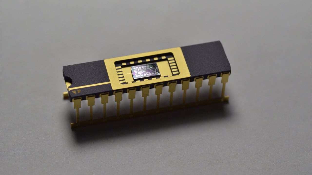
Engineer Sam Zeloof has become, to common knowledge, the first person to successfully create an integrated circuit using a fully photolithographic process in a home lab, building a dual differential amplifier using entirely homebrew equipment.
Hobbyists around the world have been making discrete circuits at home for years, but integrated circuits are a significantly trickier matter. Engineers like Jeri Ellsworth have succeeded in the past using conductive epoxy and other tricks for the on-chip interconnects, but Sam’s work is the first to use a photolithographic process – the means by which modern IC are created, traditionally involving an expensive cleanroom environment with even more expensive photolithographic equipment.
In a write-up of Sam’s achievement on Hackaday, the process is explained in brief: use of a converted digital light panel (DLP) projector for ultraviolet photolithography and an electron microscope for electron-beam lithography, and sputtered aluminium for on-chip interconnects. While still not exactly within reach of your average hobbyist, Sam’s work demonstrates that it is possible – with time and ingenuity – to build photolithographic ICs in a garage environment.
The news comes just one day after OnChip unveiled the second generation of Itsy-Chipsy, an IC fabrication platform which aims to allow hobbyists, tinkerers, and prototypers access to professional low-count IC fabrication for as little as $100 per chip.
More information on Sam’s work, not yet including a full write-up of his first successful IC output, is available on his personal blog.

Gareth Halfacree is a technology journalist and technical author best known for his work on the Raspberry Pi User Guide and an upcoming book covering the BBC’s micro:bit project. A keen open source advocate and RISC-V fan, Gareth is responsible for curating our fortnightly community round-up posts.